SRM-20 / How to make a LED circuit board

Created Date: 2015-07-03/ updated date: 2018-03-13
    Owner & Collaborators
    License
    Summary
    FabLab Kamakura has held CNC milling machine classes for beginners. This page is a summary of that class. 
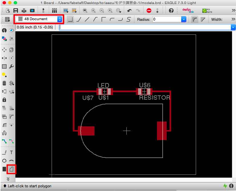
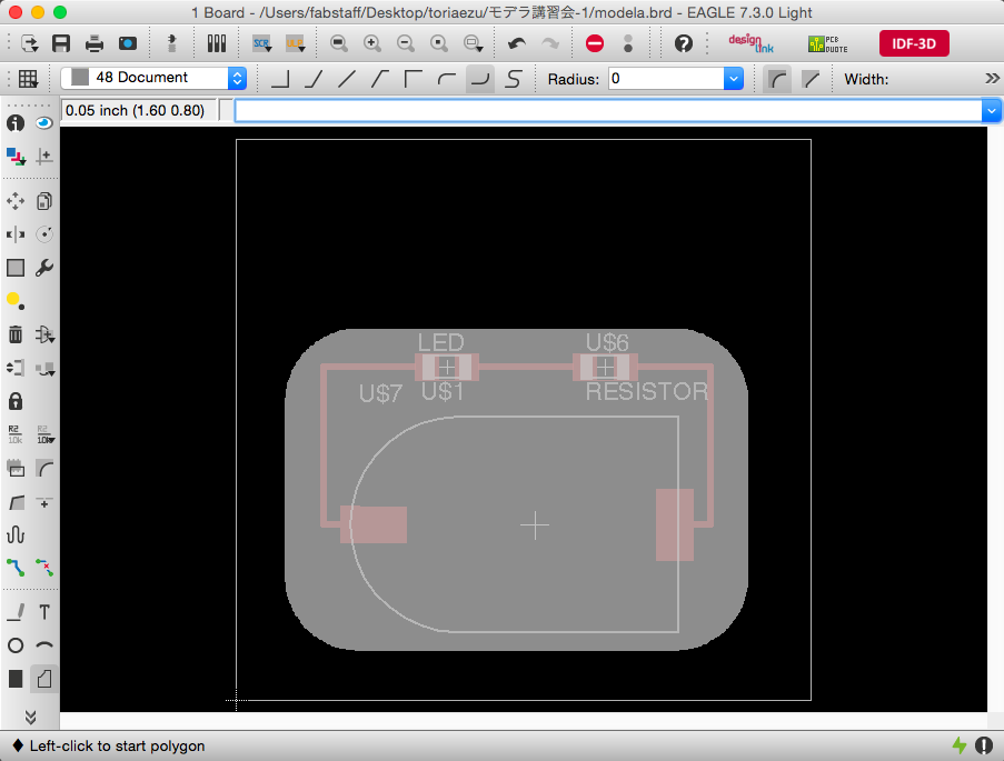
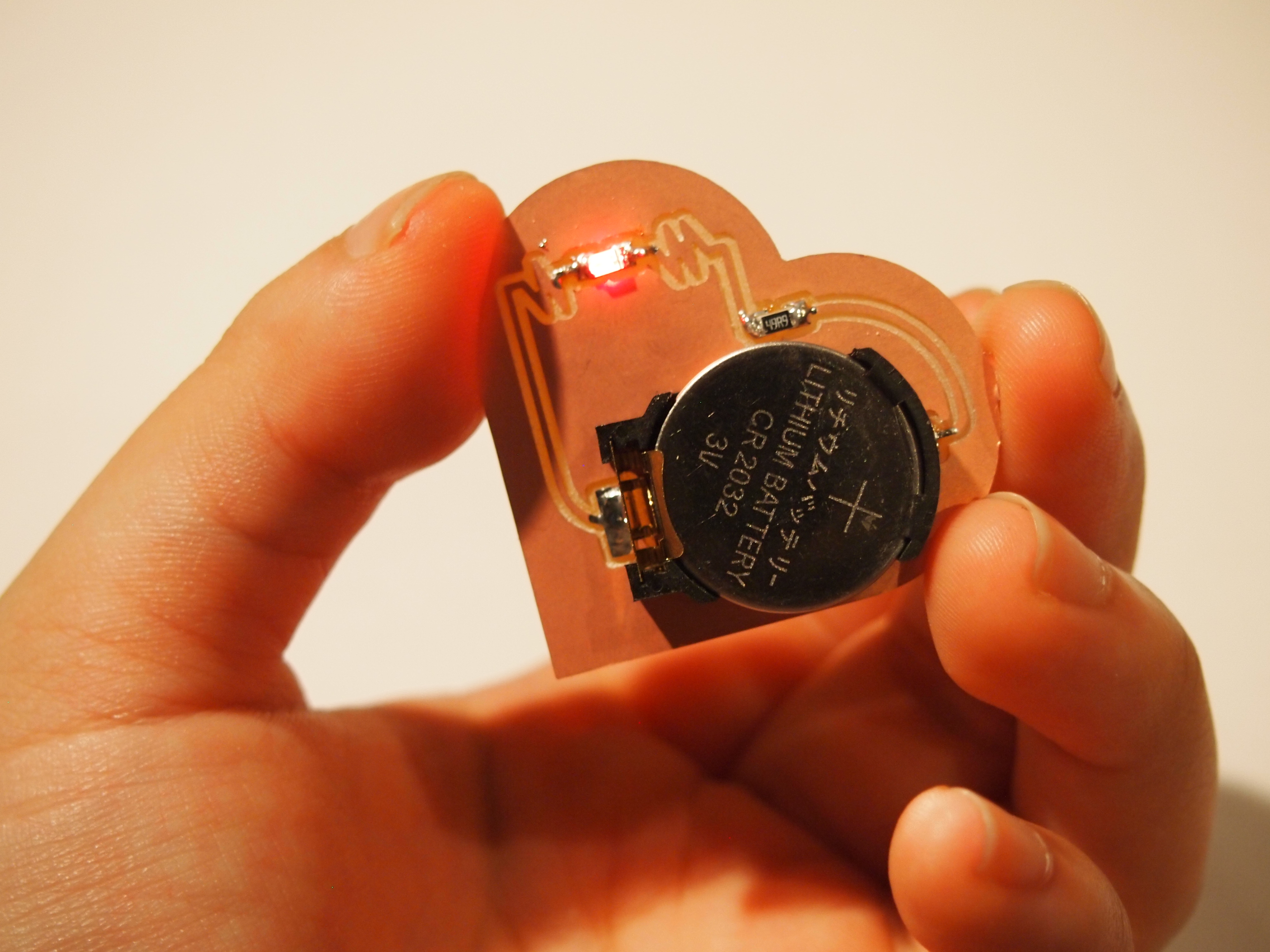
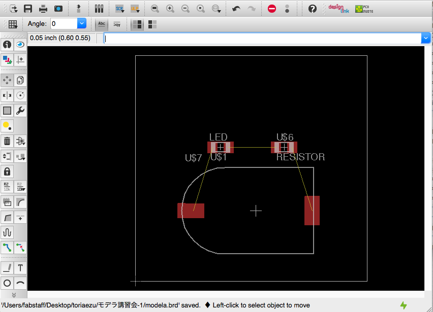
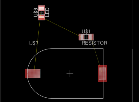
In this tutorial you can learn how to make a simple circuit board with a LED.
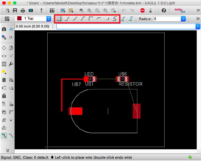
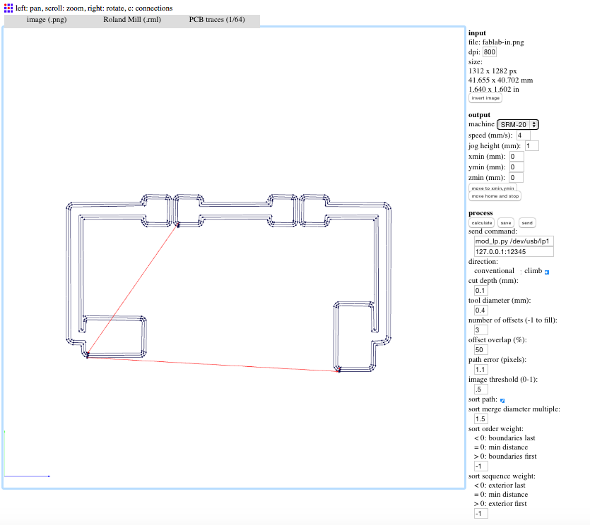
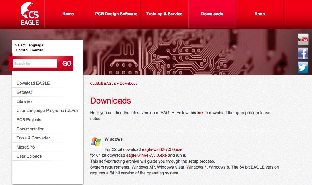
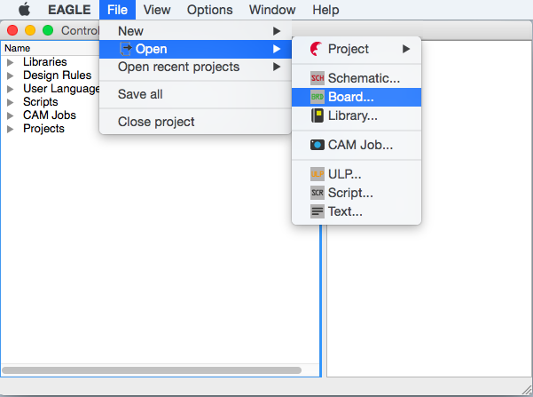
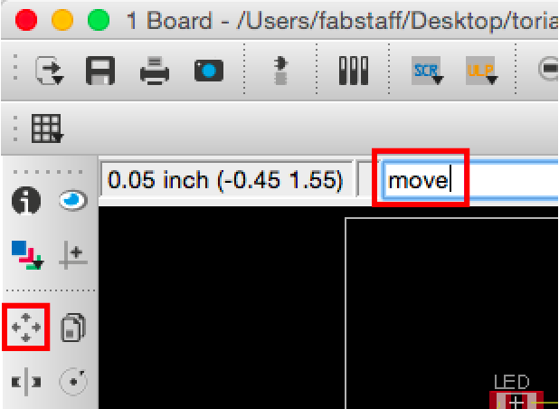
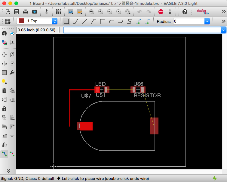
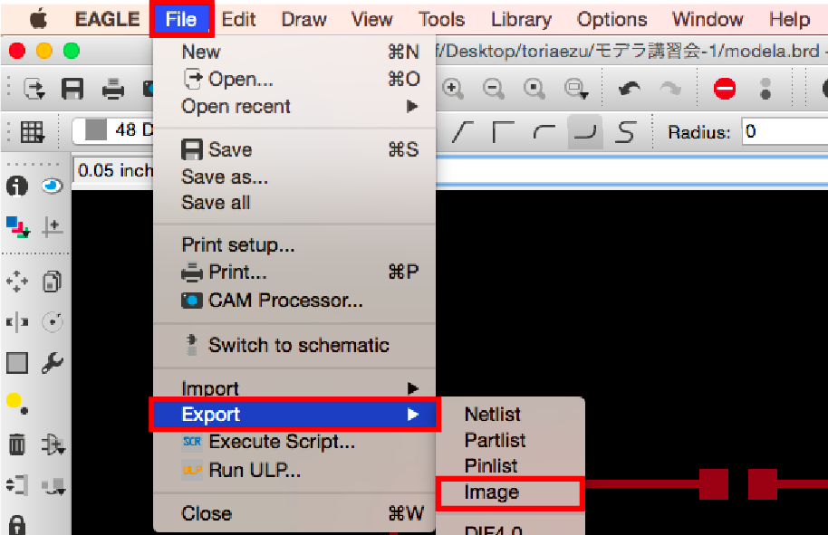
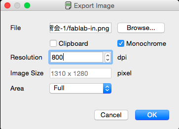
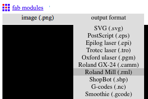
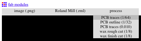
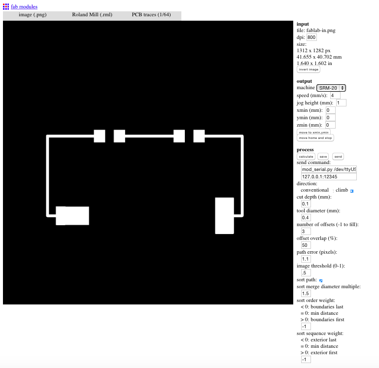
    We explain how to make the circuit data using a software called Eagle, and how to mill the circuit board using the milling machine (SRM-20).

    Materials

      Tools

        Blueprints

          Making

          • Here we explain how to make the circuit data for the LED.
            • Decide where to place the battery box, LED, and resistor. 
              There is a command line at the top of the window. 
              Type in “move”, press Enter and click the components to move them.
              (Or you can click the [move command] on the toolbar at the left side of the window)
            • When you have finished arranging all of the components, wire them together. 

              Execute the Route command to connect each of the components’ pins. 
              Once you click one end of a component, the end of another component will be highlighted. Click and create a path to connect those ends.

            • First, connect the negative end of the LED to the negative end of the battery box.

              ※ Do not click and drag. Just click.
              ※ Be careful not to double-click or the wiring will stop at that point.
              ※ Make sure that the red lines DO NOT cross over.
            • Connect the rest of the components.

              ・Positive end of the LED → One end of the resistor
              ・Other end of the resistor → Positive end of the battery box.

              ※ If you want to change the angle or curve of the wiring,
              right-click during wiring, or use the toolbar at the top of the window.
            • If you want to erase the wiring, execute the Rip Up command and click the wire.

            • Execute the Polygon command by typing "Polygon" or clicking the [Polygon command].

              From the top of the window, change the layer form [1 Top] to [48 Document]

              ※ The outline of the board has to be saved on a different layer in order to save it separately from the other data,
            • Draw the outline by clicking several times.

              When the beginning and end of the line is connected, the inner area will turn into a transparent white color and the shape will be finalized.

              ※ If you press ESC before the shape is finalized, all of the lines will be erased.

            • Now, we will export the PNG file of the circuit's traces.

              Execute the Layer command and select [None] to deselect all of the layers.

              Select the numbers of [1 Top], [17 Pads] and [18 Vias] to show only the traces of the circuit, and press [OK].
            • From the menu at the top of the screen,  select [File] → [Export] → [Image] to export the circuit’s data.

              Browse and select the place to save the file, type the file’s name and save it as a png file.

              Check [Monochrome], change the resolution to [800 dpi] and press [OK] to save.
            • Select only the [48 Document] layer and repeat the steps from [Export to png(2)] to save the outline file.
          • Fab Modules is an online, open source, CAM software which we will use to convert the [.png] file to [.rml] file (path data). 

            Go to the site and follow the steps below.
            • Open an internet browser and go to the following link.
              fabmodules.org


              Click [input format] to show the extension names. 

              Select [image(.png)].

              Select the png file and click [Open].
            • Select the bit's size by clicking [process] and selecting [PCB traces (1/64)].


              ※For exporting the outline data, select [PCB outline (1/32)].
            • Click the [calculate button] located under process, to create the path data.

              Once the tool path data appears on the left area of the screen, click the [save button] to download the data.
            • Repeat steps (1) to (4) to create and save the outline’s path data.

              ※For exporting the outline data, select [PCB outline (1/32)] in step (3).
          • Here we explain how to mill the circuit board with the SRM-20.

            We will use a software called [VPanel] (provided by Roland) to export the [.rml] data.
            • Turn on the SRM-20.

              Turn on the computer that is connected to the SRM-20 and open [VPanel].
            • Here we use VPanel to set the bit’s origin.  There are two settings.
              • Machine Coordinate System
                   The preset of the bit’s origin.

              • User Coordinate System
                   The user determines the bit’s origin.

              This time we will use the User Coordinate System.
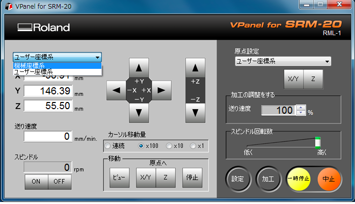
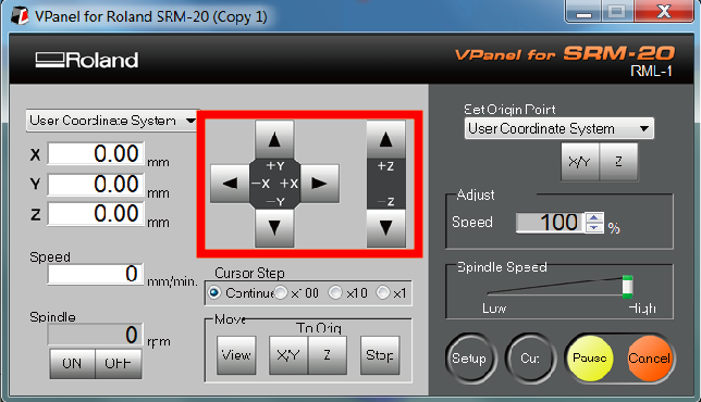
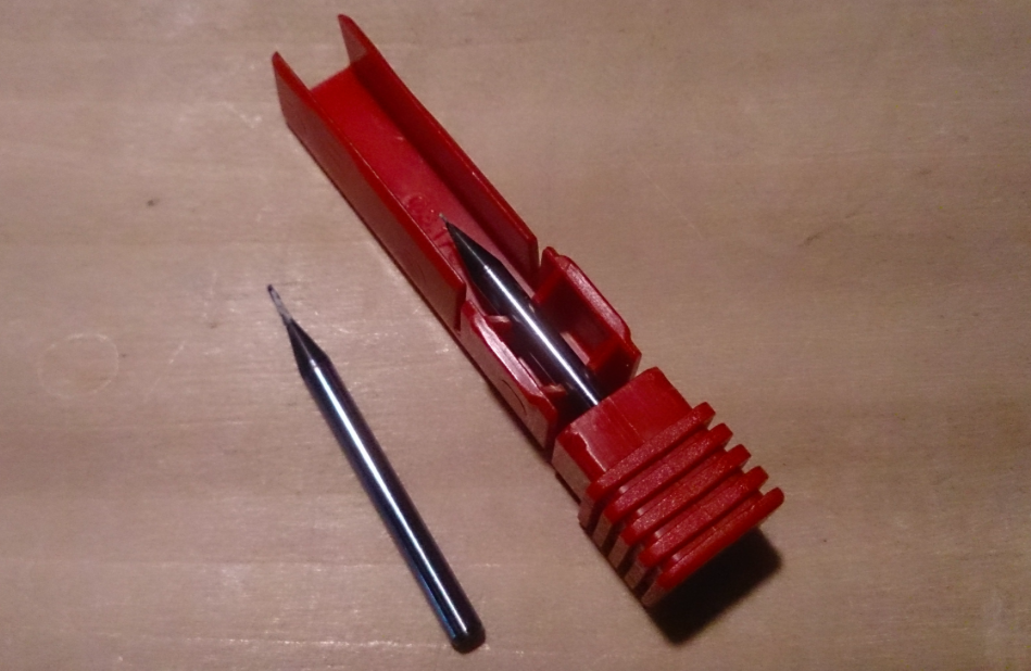
            • After inserting and securing a 1/64” bit in the spindle, click the [X/Y arrows] to set the origin of bit. Carefully click the [Z arrow] and lower the bit until it is slightly above the board. 
            • Now we adjust the bit so that it touches the board.

              While holding the bit with one hand, loosen the setscrew on the spindle with a hexagon wrench, carefully place the bit on the PCB, and gently tighten the setscrew. 

            • ※ DO NOT tighten the setscrew with too much force or you may damage it.
              ※ DO NOT drop the bit on the board or the tip may break.
            • Click [Add] and select the [.rml file] for the circuit's traces.

              When the [Output] button is pressed, the machine will begin to mill.

              ※If the previous files appear in the Output File List, delete them before opening the [.rml] file.
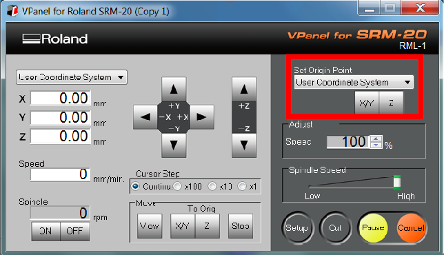
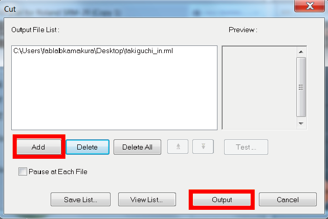
            • For the outline of the circuit board, change the bit to 1/32”. Use the [Z arrows] and hexagon wrench to adjust the bit. Then, click only the [Z button] under Set Origin Point to re-set the bit’s origin.

              ※DO NOT forget to re-set the bit’s origin ([Z button]), or the bit may break.
            • Repeat the previous steps from Send the Cutting Data for milling the outline of the board. ( [Cut] → [Add] → [Select the .rml file] → [Output] )
            • When the milling is done, open the front window, loosen the 4 screws and take out the orange stage.
            • Pour the solvent between the orange stage and the PCB. Insert the scraper between the stage and the PCB and carefully remove the board.
          • Begin to solder from the smallest components.

            [LED] → [Resistor] → [Battery case]
            ※Be careful! The LED has polarity. The side with the green line is - (anode).

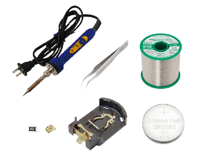
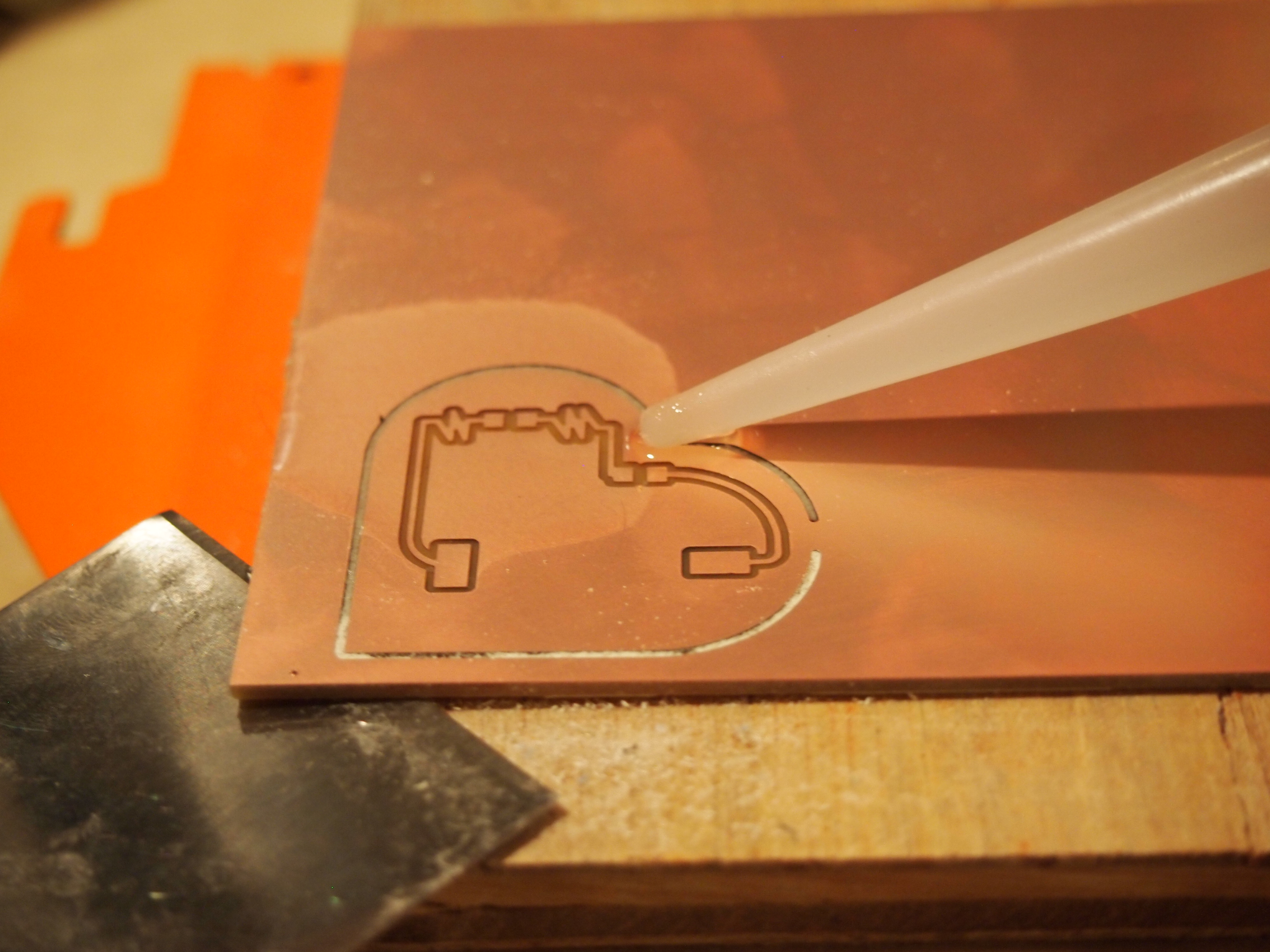
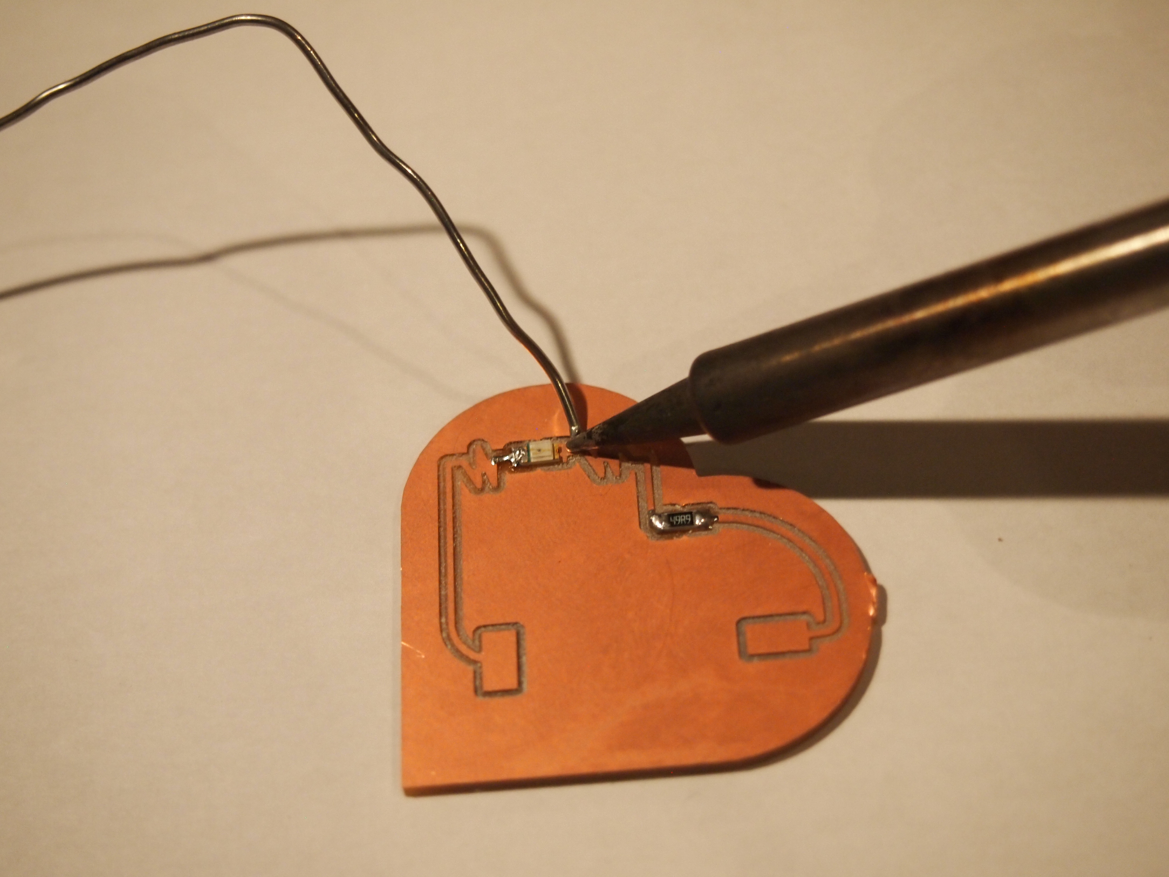
            • Flow a little amount of solder into one of the pads
              Wet the soldering iron with a little solder. Press the tip of the soldering iron on a pad. Briefly press the solder on the board and flow it on the pad. Release the solder, then the soldering iron form the pad.
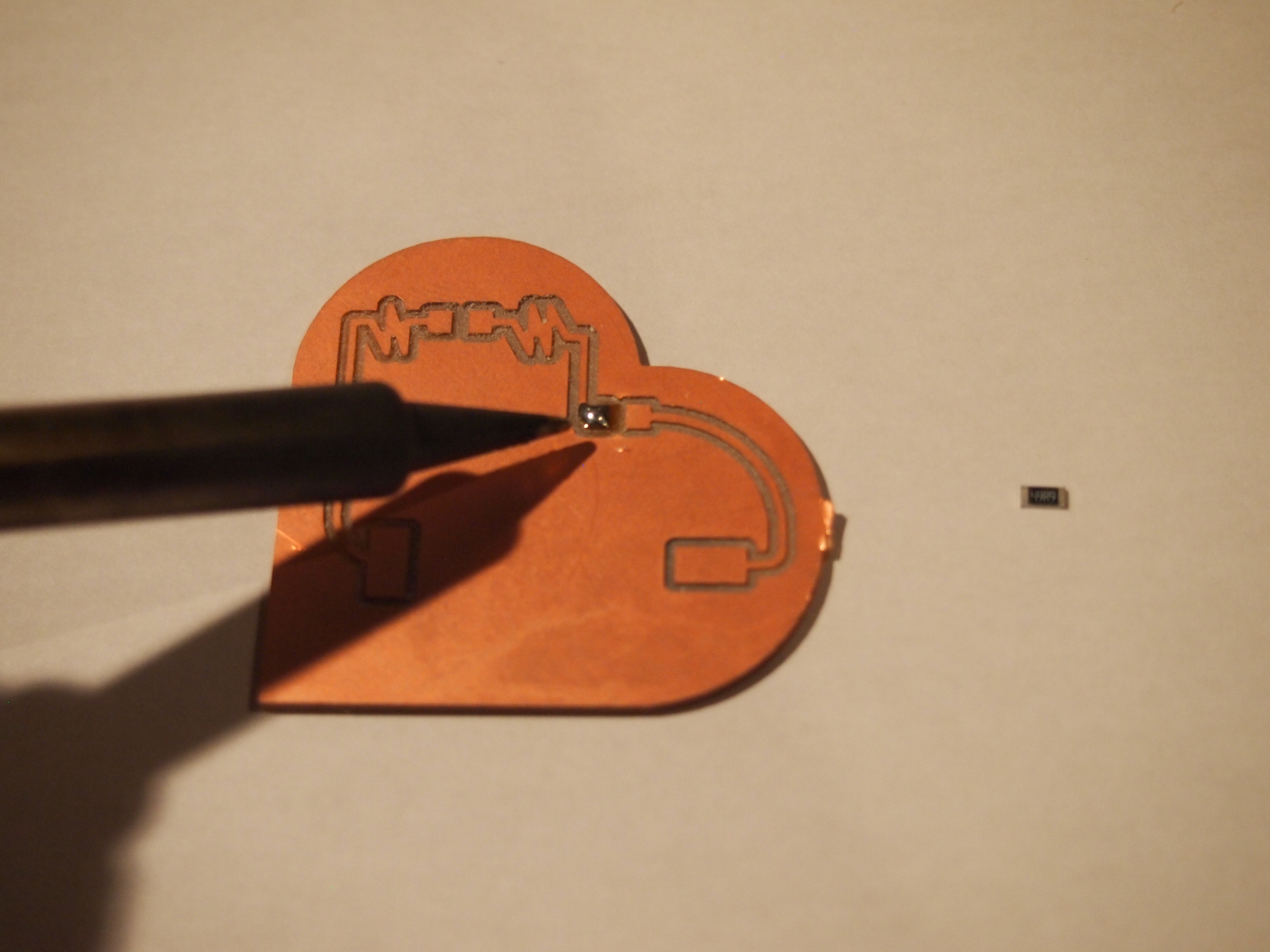
            • With a tweezer, hold the small component and press it on the soldered pad. Warm that pad until the component is connected to the board. Solder the other pad.
          • Insert the battery.

            If the LED turns on your circuit board is complete!
            • ・Press the tip of the soldering iron on the board and warm it up before flowing in solder.
              ・Turn off the soldering iron whenever it isn’t being used.

          Add Card Order

          References

            Usages

              Project comments

              • No.001suman01Posted date: 2023-10-27
                Cheap Goa Call Girl wherein you may come upon good-looking unbiased call women of all paperwork, dimensions.